The Yan lab’s research goal is to understand atomic- and nanoscale physical and chemical phenomena in materials, and establish the correlations among structure, process, properties, and performance of low-dimensional materials. Our approach employs a combination of materials synthesis and advanced ex-situ and in-situ characterization via scanning/transmission electron microscopy (S/TEM).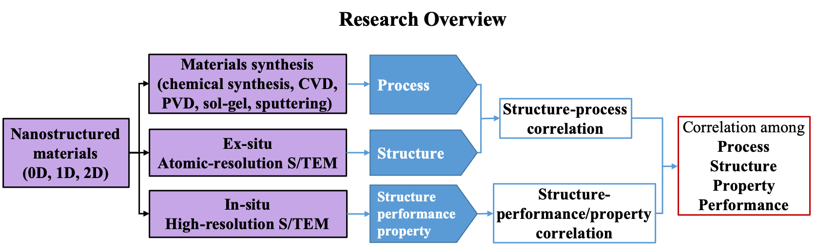
Level 1: Atomic-/nanoscale structural and property engineering via materials synthesis and high-resolution ex-situ S/TEM characterization
Two main categories of nanostructured materials are: (1) materials with one or more dimensions confined to less than a few nanometers. Examples are nanoparticles (zero-dimensional or 0-D materials), nanowires/nanotubes (one-dimensional or 1-D materials), and layered sheets (two-dimensional or 2D materials); and (2) bulk materials with building blocks that have nanometer characteristic length scales. These nanoscale building blocks significantly impact the macroscopic properties of the material (such as alloyed crystallites with nano-sized domains). New physical phenomena and unique properties can emerge in nanostructured materials due to their reduced dimensionality and coupling between nanoscale building blocks. Moreover, extended interfaces or/and surfaces in these nanostructured materials facilitate the flexible integration of various nanoscale components with different properties. This enables new functionalities that are impossible with each individual component. Additional degree of freedom in designing materials with desired properties can be achieved by engineering interfaces and structural defects (such as point defects, dopants, dislocations and grain boundaries) in these nanostructured materials. This is because these structural components can significantly affect the materials’ optical, electrical and mechanical properties. Among nanostructured materials with different dimensionalities, atomically thin 2D materials are especially attractive because of their outstanding physical and chemical properties and numerous members with diverse nature. Additionally, the weak van der Waals force that binds layers in 2D materials enables the flexible combination of different 2D materials and allows for the implementation of other 0D and 1D structures, yielding an integrated system with novel functionalities that can be designed and tailored.
To create these nanostructured materials, we use methods such as chemical vapor deposition (CVD), physical vapor deposition (PVD), bottom-up sol-gel techniques and various sputtering methods (such as thermal sputtering and electron beam sputtering). We also apply various defect engineering strategies (such as plasma treatment, laser beam treatment and surface functionalization) to further modify the materials’ properties. The newly synthesized nanostructured composite systems will have potential applications in numerous fields, such as next-generation flexible devices, high-efficiency catalysis, optoelectronics, biological sensing and electrochemistry. Although these synthesis methods are flexible for making different nanostructured materials with high productivity, they are known for their complexity in choosing the right synthesis parameters and difficulty in controlling the process. It will be even more challenging to achieve reproducibility and controllability if multiple nanostructured materials are to be interfaced or integrated via a sequence of different synthesis processes. To overcome these challenges, we will establish a strong synthesis-structure correlation for different nanostructured materials by characterizing their structure and properties via high-resolution ex-situ S/TEM. This unique approach of combining synthesis and structural/property characterization will enable a comprehensive understanding of the correlation among growth mechanisms, microstructure and properties of as-synthesized nanostructured composite material systems.
Level 2: In-situ/operando S/TEM study of nanostructured materials and their composite systems for real-life applications
Nanostructured materials and their composite systems have great potential in various applications such as ultra-thin and flexible transistors, lithium ion batteries and catalysis. In these real-life applications, materials work under different external stimuli, such as varying temperatures, electrical biasing, mechanical deformation and local chemical reaction. These environmental stimuli can significantly impact nanostructured materials and their composite systems because of the multiple surfaces/interfaces that are prominent in these systems. Additionally, the local atomic structure such as surfaces, interfaces and defects can determine/control the macroscopic performance of materials under different environment. High-resolution S/TEM is an ideal tool to study size-dependent structural and property evolution of nanostructured material systems under different external stimuli. This is because S/TEM has fast data acquisition capability, and various characterization length scales (from sub-angstrom to micrometer).
Among all the external stimuli mentioned above, heating, electrical biasing, and mechanical deformation can be readily integrated into an in-situ TEM holder, and applied to materials of interest in high vacuum (normal S/TEM operating mode). Other stimuli such as chemical reactions in liquid/aqueous electrolyte inside an electrochemical cell or in a gaseous environment for catalysis, can only be applied in non-vacuum S/TEM, or environmental S/TEM. Our research focuses on the above in-situ/operando S/TEM schemes to study the dynamics in different nanostructured material systems for applications in devices, electrochemistry, biological imaging and catalysis.